
Glass Core Substrate Sector Research: Part 1
By Jin

About two months ago, we published our first article on glass substrates and glass interposers.

In six articles, spread over the next two weeks, we’re going to dive deeper in the sector and talk about the technology behind glass core substrates, why ABF substrates are running out of road, the full supply chain of who's building what, and our framework for timing the investment as the sector moves toward high-volume production around 2030.
In this part
• Executive Summary
• 1. Problem Definition: Why Glass Is a Live Topic
• 2. The AI Packaging Stack
• 3. Interposer Evolution and the Timing of CoPoS Adoption
Executive Summary
Investing in glass substrates for advanced packaging at this point in the cycle is a bet whose outcome turns sharply on the timing of commercialization. This research sets out our base scenario for that timing and a quarterly signal framework for monitoring whether that scenario is unfolding on schedule.
Glass enters advanced packaging in two distinct layers: the interposer layer that connects die to die, and the substrate layer that supports the entire package. The adoption conditions for the two paths are fundamentally different. Our conclusion is that the first entry point for meaningful revenue is on the glass core substrate side. Glass interposer revenue at scale requires the separate precondition of mass production entry for TSMC’s CoPoS (Chip on Panel on Substrate, an interposer process built on rectangular panels rather than round wafers), and we estimate that production timing at no earlier than around 2030. Glass core substrates, by contrast, face adoption pressure from the physical demand of package area expansion alone, and multi-customer sample activity is already observable across AMD, Apple, Broadcom, AWS, and Intel.
Our base timeline scenario places glass core substrate entry into high-volume manufacturing (HVM) in 2030. Our bear scenario places this at 2031 to 2032, one to two years behind. The four to five most advanced glass substrate manufacturers are currently in stages 3 to 4 of an internal 10-stage production readiness model, while chip design customers are in stages 5 to 6 of a separate 14-stage model. The decisive inflection point over the next 12 to 18 months is therefore whether glass substrate manufacturers enter stage 5 (specification freeze). Until that entry is confirmed, we believe the investment risk is not meaningfully resolved.
The progress signals we track each quarter cluster into four areas: (i) qualification and reliability pass references in earnings calls and IR materials; (ii) external customer commitments for Intel EMIB-T and progress at TSMC’s CoPoS pilot line; (iii) capex signals beyond R&D from Absolics and Samsung Electro-Mechanics, as well as from ABF substrate incumbents such as Unimicron and Ibiden; and (iv) concurrent rather than single-vendor backlog increases at equipment suppliers including LPKF, Philoptics, and E&R Engineering.
Bottom Line
There is a four-year gap between the timing that the market has already priced in and the point at which meaningful revenue actually arrives. If evidence of glass substrate adoption in next-generation chip designs is confirmed within 2027, the narrative has room to re-accelerate. If that evidence is thin, or if ecosystem company quarterly results fall short of consensus, the expectations already in the price unwind and the near-term correction risk is material. We view 2026 as still a risky year for glass core substrate investment. A signal-based, phased approach is how AAIG is positioning, given the timing risk.
Evidence Tier Notation
Throughout this report, AAIG Verdict boxes and supply-chain summary tables tag load-bearing claims by source tier. The notation is as follows.
[T1] First-party source. Company filings (10-K/10-Q, IR materials), earnings call direct statements, official press releases, publicly demonstrated samples, board resolutions.
[T2] Reputable secondary. Tier-one sell-side notes (Goldman Sachs, JP Morgan, Morgan Stanley, UBS, Bank of America), industry research (Yole, TrendForce, Future Markets Inc.), established trade publications (DigiTimes, Nikkei, ETNews, Tom’s Hardware).
[T3] Unverified or weakly sourced. Secondhand reporting, “reports indicate” without named source, persistent industry rumors, single-source claims not corroborated. Conclusions resting primarily on T3 evidence carry correspondingly lower confidence.
[AAIG est.]. AAIG-derived estimates or working assumptions, distinguished from sourced facts. Used for analyst-built numbers (e.g., 2030 cost gap, scenario probabilities) that are anchored to sourced inputs but synthesized by AAIG.
1. Problem Definition: Why Glass Is a Live Topic
1.1 Capital Eventually Lands on Chips and Packaging
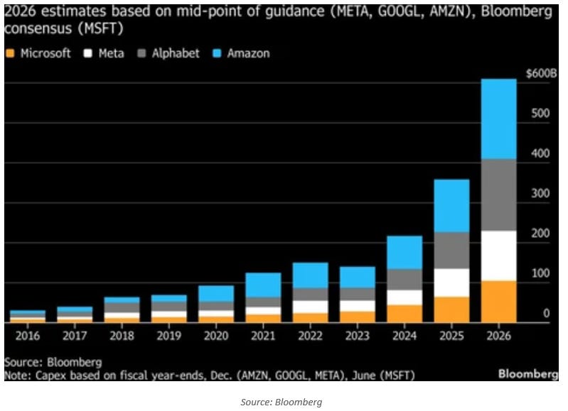
Hyperscaler capex in 2026 will comfortably exceed USD 600 billion, and the majority of that capex is concentrated in AI infrastructure. If we trace where this capital ultimately flows, the destination is chips and the packaging process that contains them. As training-driven workloads give way to inference and autonomous agent workloads, AI accelerators are being redefined: the problem is no longer how to make a chip faster, but how to fit more chips and more memory into a single package.
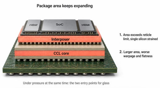
This pressure lands on two layers. The first is the interposer, the intermediate layer with fine wiring that connects chip to chip. The second is the substrate, which supports the entire package. The starting point of this research is the observation that both layers are under pressure at the same time.
1.2 Packaging: From Single-Die to Multi-Die Integration
For more than a decade, gains in chip performance came primarily from drawing circuits more finely within a single die. That paradigm has shifted. As the efficiency of further on-die shrinkage hits diminishing returns, the focus has moved toward integrating multiple dies into a single package. A graphics processing unit (GPU), high-bandwidth memory (HBM, vertically stacked memory architecture optimized for throughput), and I/O dies are now combined inside one package.
The implication is simple. Packaging is no longer a finishing step after the chip is made. It has become a core layer that determines system performance itself.
1.3 Over Time, Limits Surface Simultaneously in Both Interposer and Substrate
We separate the limits by layer.
Interposer layer limits. The interposer was once the dominant bottleneck. Fine wiring density and signal integrity were the core problems. TSMC’s Chip on Wafer on Substrate (CoWoS, a 2.5D packaging approach in which dies are attached to an interposer on a round wafer and then mounted on a substrate) has pushed these limits forward in stages. As package area moves several multiples beyond the reticle limit (the maximum area, approximately 858 mm², that can be patterned in a single exposure), strain accumulates in the very approach of building a single silicon interposer.
Substrate layer limits. This is the more recently re-emerging bottleneck. The substrate is responsible for the mechanical stability of the entire package and for thermal deformation. As packages grow larger, three problems appear at the same time. First, warpage caused by mismatch in coefficient of thermal expansion (CTE, the rate at which a material expands per degree of temperature increase). Second, the difficulty of maintaining flatness over a large area. Third, mechanical deformation when rigidity is insufficient.
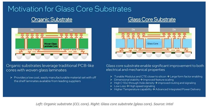
The existing substrate, more precisely a stack of Ajinomoto Build-up Film (ABF) layers laminated on a Copper Clad Laminate (CCL) core, has historically responded with reinforcement: substituting T-glass for standard glass cloth, adding stiffeners, and balancing CTE through design. These measures buy time at incremental cost. They do not change the underlying structure.
1.4 Why Glass Is Back on the Table
As limits surface in both layers simultaneously, glass has re-emerged as a candidate material. Glass can appear in both layers:
Glass interposer. Replacing the redistribution layer (RDL, the fine wiring layer formed on top of a chip or interposer) on a silicon-based interposer with one built on glass.
Glass core substrate. Replacing the CCL core in the substrate layer with a glass core. Glass provides the structural support for the entire package.
The two paths are connected but their adoption timing and inevitability are not the same. Conflating them breaks the investment analysis. That is the starting hypothesis of our work.
1.5 Where Does the Glass Interposer Stand in Current AI Chip Packaging?
In the interposer layer, glass is recognized for its long-term necessity but is not on a near-term path to broad adoption. Glass interposer also targets the high-performance packaging market, but the realistic adoption path is not straightforward. Intel’s main approach is EMIB-T, which omits the interposer layer entirely. TSMC has not signaled an attempt to introduce a glass interposer into its existing CoWoS platform. The possibility that a glass interposer appears in a new TSMC packaging variant has been raised, but it remains a possibility rather than a roadmap commitment.
On TSMC’s Q1 2026 earnings call, Chairman C.C. Wei publicly confirmed a CoPoS pilot line, an approach that builds interposers on rectangular panels rather than round wafers, and described mass production as occurring “a couple of years later.” DigiTimes is more conservative: citing process uniformity and warpage issues, it lays out a scenario in which mass production slips roughly two years from the prior expectation, with the first production batches arriving in Q4 2030.
An important distinction is required here. The introduction of CoPoS does not automatically mean the panel material becomes glass. CoPoS is more likely to start with organic panels. Although glass has clear advantages on large-area interposers like CoPoS, a full transition to glass requires the CoPoS process infrastructure to stabilize first. The likely path is therefore an organic start, with large-scale glass interposer adoption lagging CoPoS mass production itself.
Glass interposer targets the high-performance packaging market, but we view the passive-substrate path here as slow to commercialize. The more practical near-term applications (Active) are in adjacent markets: 5G/6G, high-frequency communications, optical interconnect, sensor packaging, medical, and specialty industrial. Covering these in full would expand the research scope considerably, so we limit our depth analysis to the latest AI accelerator and packaging context. We note, however, that the lower layers of the ecosystem (equipment, materials, raw glass) are substantially the same across glass core substrate and glass interposer. When investing in equipment, materials, or raw glass plays, the glass interposer TAM should be factored in as well.
1.6 Where Does the Substrate Layer Stand in Current AI Chip Packaging?
The substrate layer is different. Once package area passes a threshold, the region where existing organic materials cannot keep up becomes progressively more pronounced. In this region, switching the core to glass is not incremental reinforcement, but a structural replacement. The current industry consensus is that the need for glass becomes salient as TSMC’s interposer area approaches 9.5x reticle. Because TSMC interposer size directly pulls substrate and package size, this is particularly relevant.
One caveat is worth flagging. The transition from structural pressure to clean material replacement is not automatic. At the chip design stage, designers first attempt to circumvent the constraint by partitioning into multiple smaller dies or by modularization. This does not mean glass becomes unnecessary, but in conditions where glass is hard to commercialize, the workaround route cannot be excluded. Adoption of glass core substrates will likely be segment by segment, occurring incrementally as realistic conditions per segment are satisfied. Glass is not avoided by preference, but constrained by practical conditions.
2. The AI Packaging Stack
2.1 Why Start with the Packaging Stack
Understanding why substrate and interposer are under simultaneous pressure requires looking first at how an AI accelerator package is constructed. The package is not a single component but a stack of layers. Separating which layer does what, and where pressure accumulates, is what reveals where glass is needed.
2.2 The Four-Layer Structure of a Modern AI Accelerator Package
A modern AI accelerator typically consists of four layers stacked vertically, with some variation. Working from bottom to top:
Layer 1: Printed Circuit Board (PCB). The main board at the bottom, which receives system power and signals. The package sits on top.
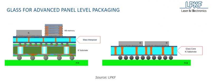
Layer 2: Substrate. The supporting structure for the package, which sits on the PCB. It carries the entire package and connects external PCB signals to the chips inside. The glass core substrate addressed in this research belongs to this layer.
Layer 3: Interposer. The intermediate layer above the substrate. It connects chips such as GPU and HBM with short, fine wiring. Glass interposer belongs to this layer.
Layer 4: Die. The actual silicon with circuitry. GPU dies and HBM stacks sit on top of the interposer.
Of these four layers, the PCB and the die are outside the scope of this research. Our focus is on the middle two layers: substrate and interposer.
2.3 Why Both Layers Are Under Pressure Simultaneously
The interposer is responsible for fine wiring and signal characteristics. As AI accelerator performance rises, the connection between GPU and HBM must become shorter and faster. When the number of HBM stacks rises and die-to-die connections multiply, the interposer’s own wiring density and area grow in parallel. As area grows, it crosses the reticle limit, and the strain on the existing process built on round wafers compounds.
The substrate must support both the interposer and the dies above. When the interposer above grows, the substrate that supports it grows as well. As the substrate grows, two problems scale non-linearly. First, thermal deformation: for the same CTE mismatch, the deformation distance scales with area. Second, the warpage of a large package transmits cumulative stress to fine solder bumps (the small metal contacts that connect die and substrate) and copper pillar connections, surfacing over time as a reliability problem.
Larger interposers imply larger substrates, and the limit in one layer pulls the limit in the other.
2.4 The Two Layers Pose Different Problems
The critical point is that the two layers do not face the same kind of problem.
The interposer layer. The dominant problem is the limit of miniaturization: how fine the wiring can be drawn. Area and cost limits are entangled with it. The candidate solutions are the process shift from round wafers to rectangular panels (CoPoS) and the material shift of that panel to glass.
The substrate layer. The dominant problem is the structural limit: maintaining flatness and mechanical stability over a large area. The candidate solution is replacing the CCL core itself with a glass core.
This difference matters. For the interposer, the glass path opens only after an additional process condition (CoPoS) is satisfied. For the substrate, glass becomes a direct answer the moment package area crosses the threshold. The conditions for the two paths differ, and so do their adoption timelines.
3. Interposer Evolution and the Timing of CoPoS Adoption
3.1 A Brief Overview of Interposer Evolution
Understanding interposer evolution starts with the reticle limit, the maximum area in which a pattern can be drawn in a single exposure. An EUV scanner (Extreme Ultraviolet scanner, equipment that uses very short wavelength light to pattern fine circuits) can pattern roughly 858 mm² in a single exposure. This is a physical limit set by optics; it cannot be raised at will.
As AI accelerator interposer area began crossing this ceiling, the reticle limit became a central constraint on package design. Even if a larger interposer is desired, the single-exposure area is fixed, and the existing approach cannot proceed unchanged. The principal question of advanced packaging research over the past several years has been how to circumvent this limit.
3.2 How TSMC Has Pushed the Limit: CoWoS Evolution
TSMC has advanced the limit in stages. The earliest form of Chip on Wafer on Substrate, CoWoS-S (S for Silicon, indicating a silicon interposer base), supports interposer area up to roughly 3.3x reticle, or about 2,700 mm². Beyond 3.3x, the recommended approach shifts to variants below.
CoWoS-L (L for Local Silicon Interconnect) is one such variant. Small silicon bridges are inserted only in regions that require high-density connections, while the remaining regions use RDL (Redistribution Layer, the fine re-wiring layer). The hybrid structure reduces the yield burden of fabricating one large silicon interposer while supporting larger areas.
On TSMC’s roadmap, CoWoS-L at 5.5x reticle (roughly 4,719 mm²) was targeted for 2025 to 2026 launch with support for 12-Hi HBM4 stacks. The next stage, approximately 9.5x reticle, is scheduled for validation completion in 2027.
In May 2026 TSMC unveiled additional CoWoS roadmap items beyond 9.5x reticle. In 2028, a 14x reticle option with support for 20 HBM5/5E stacks was disclosed, an aggressive projection. On the surface, this appears to suggest CoWoS can be extended at reticle multiples without bound, but practical difficulties remain significant. We discuss these in the next subsection.
3.3 The Area and Efficiency Limits Confronting CoWoS-L
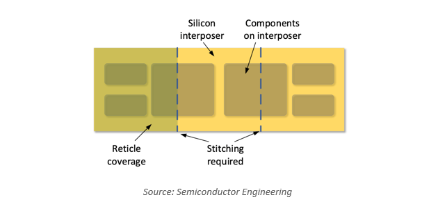
CoWoS-L is hitting its own limits as area grows. The essential nature of this limit is not a simple material constraint but an efficiency limit of the round wafer format itself.
CoWoS-L builds interposers on round wafers. As interposer area grows, the number of interposers that can be made from one wafer decreases. The corners of a round shape leave regions unsuitable for cutting out rectangular interposers. This edge loss is negligible when interposers are small, but the loss ratio rises sharply when a single interposer exceeds 5,000 mm² and moves into the 7,000 to 8,000 mm² range.
From a productivity standpoint, the conclusion is straightforward. A format that produces more interposers per cycle is required. The transition from round wafers to rectangular panels is the natural answer. Rectangular panels have small edge loss, and at the same installed area they deliver more usable area than a comparable wafer. This is the most direct reason CoPoS has emerged.
3.4 Why Glass Enters the CoPoS Discussion
When CoPoS scales up the panel, a new problem becomes pronounced. The CTE of organic panel materials is roughly 20 to 50 ppm/°C (parts per million per degree Celsius, the proportional expansion per degree of temperature rise). The CTE of a silicon die sitting on the interposer is approximately 3 ppm/°C, a difference of roughly an order of magnitude.
Over small areas, this difference is not a problem. Once the panel scales up rectangularly, the story changes. Even with the same CTE mismatch, the absolute difference in expansion distance grows with area, and that difference manifests in two ways.
First, drawing fine wiring (RDL) on the interposer requires precise alignment. If alignment drifts while the panel expands and contracts thermally, the precision of fine RDL breaks down.
Second, when a large panel warps or deforms, the achievable circuit density on top of it is limited. Larger panels imply lower achievable precision unless the underlying CTE issue is resolved.
Resolving both requires the panel material’s own CTE to be close to that of silicon. Glass has a CTE of roughly 3 to 5 ppm/°C, very close to silicon. Even over large areas, it expands at nearly the same rate as the silicon die, reducing alignment error and deformation. The result is that fine RDL precision can be maintained on large panels.
To summarize: CoPoS emerges to produce more per cycle, and glass emerges to maintain precision on the resulting large panel.
3.5 The Current Status of CoPoS
The official position on CoPoS can be summarized as follows.
TSMC official commentary. On the Q1 2026 earnings call, Chairman C.C. Wei publicly confirmed the CoPoS pilot line and described mass production as occurring “a couple of years later.”
Pilot line schedule. TSMC’s CoPoS pilot line begins equipment move-in in February 2026, with line construction targeted for completion by June.
Panel size. The most commonly cited size in press coverage is 515 x 510 mm, although some reports suggest TSMC is starting with 310 x 310 mm for strategy development before scaling up.
An important distinction is required. TSMC officially mentioning CoPoS is not the same as TSMC officially stating direct integration of CoPoS with a glass interposer. The latter has not appeared in any official TSMC communication. The “longer-term goal” phrasing referenced by industry outlets such as Commercial Times is industry observation, not a TSMC roadmap announcement.
3.6 CoPoS Mass Production Timing: Two Coexisting Scenarios
Two scenarios coexist for the timing of CoPoS mass production.
TrendForce / Commercial Times scenario. Mass production begins between 2028 and 2029.
DigiTimes scenario. Process uniformity and warpage issues push mass production out by roughly two years, with the first production batch arriving in Q4 2030. The sequence is: R&D equipment move-in in Q3 2026, pilot equipment orders in Q3 2027, pilot equipment installation at Chiayi P7 in Q2 2028, mass production equipment orders in mid to late 2029, and the first mass production batch in Q4 2030.
Whether the gap between these two scenarios narrows or widens is one of the key indicators to watch going forward. We refer to this as the “two CoPoS scenarios” framework.
Through March 2026, the weight was on the DigiTimes scenario (Q4 2030 mass production). More recent Chinese press reports indicating that TSMC is actively considering three CoPoS facilities in Longtan, together with the visible intensification of competition with Intel, have shifted the balance: a CoPoS schedule earlier than the DigiTimes bear case is becoming more plausible. The 2028 roadmap entry for 14x reticle CoWoS should also be read as an accelerator signal for CoPoS, since the two compete in a closely related design space. Weighing TSMC’s acceleration factors against the process uniformity and warpage realities flagged by DigiTimes, we set our base CoPoS mass production timeline at H2 2029 to 2030.
3.7 What Happens If CoPoS Mass Production Slips
If CoPoS mass production slips into 2030 because of technical problems, three structural consequences follow.
First, the strategic life of CoWoS is extended. If CoPoS does not enter mass production before 2030, almost all AI accelerator packaging demand from 2027 to 2030 must be absorbed by CoWoS, particularly CoWoS-L. As we discuss further, this is close to impossible in practice, and TSMC has strong incentives to bring CoPoS to mass production as soon as possible.
Second, large-scale glass interposer adoption is delayed in tandem. Mass adoption of glass interposers requires both CoPoS adoption and precision maintenance on top of it. If CoPoS mass production slips beyond 2030, large-scale glass interposer adoption slips further still. Even when CoPoS arrives, panels do not automatically shift to glass: an organic panel start is more likely.
Third, paradoxically, the relative importance of glass core substrates rises. As the interposer layer’s material transition is pushed beyond 2030 and TSMC stretches CoWoS to enlarge interposer area, the mechanical stability problems from package area expansion surface first in the substrate layer. This is the central reason our analysis focuses on glass core substrates. In particular, adoption of glass core substrates in advanced packaging appears most likely to occur on the Intel side first. Intel does not adopt glass interposers, and CoPoS mass production may slip to 2030. While glass interposer is recognized for long-term necessity, our conclusion is that it is unlikely to enter meaningful revenue tracks over the short term (three to five years).
Great write up! Wrote about same topic from my perspective
https://arvindsrinivas.substack.com/p/know-your-glass-complexity-and-importance