
Glass Core Substrate Sector Research: Part 2
By Jin

Here is part 2 of our Glass Core Substrate sector research. In the first part, we talked about problem Definition: Why Glass Is a Live Topic, The AI Packaging Stack and Interposer Evolution and the Timing of CoPoS Adoption.
In this part, we’re talking about the Core Technology: ABF Limits and What Glass Changes.
4. ABF Substrate Structure, Its Limits, and What Glass Core Substrates Mean
5. What Would It Take for the Economics of ABF and Glass to Cross?
4. ABF Substrate Structure, Its Limits, and What Glass Core Substrates Mean
4.1 Defining the ABF Substrate Structure Precisely
Discussing why a glass core substrate is needed requires precisely defining what we call the “ABF substrate.” Confusion at this point blurs the distinction of what glass actually replaces.
In contemporary AI accelerators, the ABF substrate is essentially composed of two parts.
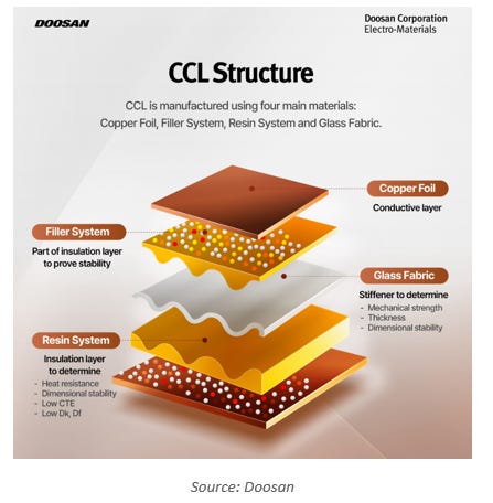
CCL Core (Copper Clad Laminate Core)
The structural backbone of the substrate. Standard glass fiber cloth (E-glass) is coated with epoxy resin to form prepreg sheets, multiple layers are stacked, and copper foil is bonded to both sides to form a rigid panel. In high-performance substrates for AI applications, T-glass, a reinforced glass cloth with a lower CTE used to suppress warpage in AI applications, is rapidly gaining share over standard glass fiber for core reinforcement. The core serves as the structural element that prevents the substrate from warping.
ABF Build-up Layer
Insulating films laminated sequentially on top of the CCL core. Each layer carries copper traces and microvias (vertical interconnects on the order of micrometers). They convert the fine bump array on the chip into larger external wiring. The build-up layer serves as the signal pathway between chip and exterior.
Together, these two parts form what is commonly referred to as the ABF substrate. “ABF” is in fact the name of the build-up film material, not the name of the entire substrate. The core is a separate CCL structure, and ABF is the insulating film laminated on top of it. The shorthand “ABF substrate” is convenient, but the precise description is a combined structure of “CCL core plus ABF build-up.”
4.2 Where Limits Surface as Package Size Grows
Of these two parts, where does the limit appear first as package area grows? The answer is the CCL core. The ABF build-up layer is affected, but it is not the root cause.
The reason lies in the difference in role. The ABF build-up layer is very thin, with each layer at the micrometer level, and is optimized for routing electrical signals between chip and exterior. The build-up layer itself does not fail simply because the package grows.
The problem surfaces in the core. Once package area enters the 100 mm plus region, the CCL core encounters three problems simultaneously and at large magnitude.
First, warpage. The overall CTE of a CCL core is roughly 11 to 17 ppm/°C. The silicon die that sits on it has a CTE of approximately 3 ppm/°C, a four to five times difference. The mismatch is manageable in small packages, but once package size exceeds 100 mm, the cumulative difference in expansion distance between the two materials causes the package itself to warp. The warpage breaks fine solder joints.
Second, flatness becomes hard to maintain. Drawing fine circuits on the build-up layer requires overall substrate flatness, but as the package grows the flatness requirement and the warpage tendency intensify simultaneously. The two requirements act in opposite directions.
Third, mechanical deformation from insufficient rigidity. As the package grows, the core begins to deform under its own weight and external stress.
4.3 ABF Build-up Survives; The Core Changes
A critical distinction follows. The transition to a glass core substrate is a partial replacement of the core, not a replacement of the build-up layer.
Intel’s 78 x 77 mm thick-core glass substrate, demonstrated at NEPCON Japan in January 2026, uses a “10-2-10” structure. The middle two layers form the glass core, and 10 RDL layers are stacked above and below. The insulating material of these RDL layers is still ABF or a similar build-up film.
Academic references corroborate the same structure. An IEEE paper treats as standard a configuration in which a 100 micrometer thick glass core is laminated with 15 micrometer thick ABF GL102 above and below. Semi Engineering’s November 2025 coverage explicitly states that the “stacked glass architecture” uses uncured ABF dielectric as an adhesive. In other words, even when glass core substrates are adopted, ABF build-up film remains in use.
The implication is simple. The glass transition does not kill the ABF market; it replaces the CCL core market in part. The role of the build-up film is preserved.
4.4 How Far Can CCL Core Reinforcement Take ABF?
If the ABF build-up layer survives, how far can CCL core reinforcement alone respond to package area expansion?
The industry has pursued four reinforcement approaches to date.
T-glass reinforcement. Replace or blend standard glass fiber (E-glass) in the CCL core with T-glass, which has lower CTE and higher elastic modulus. The structural concern is that roughly 90 percent of global T-glass supply is concentrated at a single Japanese supplier, Nittobo.
Stiffener addition. Metal or composite stiffeners are attached at the substrate edge to raise rigidity. As the package grows, stiffener size and area grow with it, raising material cost and process steps. Furthermore, the CTE mismatch between stiffener, resin, and ABF layers introduces new deformation modes, forcing whole-package CTE balancing in design. The result is additional cost.
ABF-GCP (Glass Cloth Prepreg). A composite material combining ABF build-up film with glass cloth. Dimensional stability and crack propagation resistance are reportedly improved. Fine-feature processing is more difficult, and while warpage can be reduced, the structural effect does not match what core replacement delivers.
Stacked glass structure. Retains the existing core but partially adds glass layers. This is closer to an early form of the glass transition than to true reinforcement.
The common feature across these four approaches is that all are incremental mitigation. They buy a little more time at additional cost. None changes the underlying structure.
4.5 Quantitative Comparison: ABF Substrate vs Glass Core Substrate Warpage
Quantitative data is available on how CCL core and glass core behave differently at large area.
According to Intel’s comparison data presented at NEPCON Japan in January 2026, at a 78 x 77 mm package area, the ABF substrate showed roughly 50 micrometers of warpage and the glass substrate showed roughly 20 micrometers. The difference is about 2.5x. This is a single measurement under specific test conditions and should be read as a relative indicator between the two materials rather than as an absolute number. The comparison did not specify whether the ABF reference was the traditional E-glass based ABF or a T-glass reinforced ABF; comparisons are conventionally made against the latest ABF reference. The signal we read is that even the latest ABF shows meaningful warpage at sub-100 mm package areas.
4.6 What Glass Core Substrates Mean in the Pre-CoPoS Era
Here we examine what glass core substrates mean in the Pre-CoPoS era, that is, the period before 2030 and before glass adoption in the interposer layer accelerates. The core question is whether substrate-layer glass adoption can occur before interposer-layer glass adoption is delayed.
Four signals point toward this possibility.
First, multi-customer sample flow on the chip design side. Sample evaluations of glass core substrates are underway across multiple chip designer to substrate maker combinations: AMD-Absolics, Apple-Samsung Electro-Mechanics, Broadcom-Samsung Electro-Mechanics, AWS-Absolics. The customer pipeline at the interposer layer is nearly empty in concrete terms, while at the core substrate layer it forms a multi-customer pattern with named customers.
Second, the CoWoS-L reticle multiple roadmap and its implication. TSMC’s plan to push CoWoS-L to 5.5x reticle in 2026 and 9.5x reticle in 2027 is an indirect signal that TSMC believes it can hold through that range without an interposer-layer glass transition. Within that window, however, the burden on the substrate that supports the package remains the same or grows.
Third, the NVIDIA Rubin Ultra specification downgrade reports. Reports indicate NVIDIA is reviewing a downgrade of the original single-package 4-die configuration of its next-generation data center accelerator, Rubin Ultra, to a 2+2 board-level configuration. Reports indicate the trigger was an interposer expansion attempt, but the surfaced symptom was substrate warpage. Extending CoWoS-L to a 4-die configuration caused thermal and mechanical stress to warp the package in multiple directions, breaking contact between compute die and substrate. This case is a real-time illustration of how interposer growth cascades into substrate burden. More recent reports (UBS) indicate Rubin Ultra may ship in two forms: a 2-chip version using CoWoS-L as before, and a 4-chip version likely on Intel’s EMIB-T. This is not NVIDIA’s official position, but together with persistent rumors that CoWoS-L’s warpage profile makes stable 4-die large-format packaging difficult, it indirectly shows how hard it is for TSMC to execute the CoWoS-L roadmap on schedule. Intel’s emergence here is worth tracking.
Fourth, glass core adoption in Intel’s EMIB-T platform. At NEPCON Japan in January 2026, Intel demonstrated a 78 x 77 mm package integrating EMIB with a thick-core glass substrate. This is a case of substrate-layer glass adoption ahead of interposer-layer glass adoption.
Taken together, these four signals point to a conclusion: glass core substrates can be adopted ahead of interposer-layer glass, with Intel as the lead adopter. That said, the conclusion that it can happen and the question of when meaningful revenue actually arrives are distinct. The intermediate stages, and how they progress quarter by quarter, are the central object of monitoring in this research.
AAIG Verdict
What we call the ABF substrate is precisely a combined structure of a CCL core and an ABF build-up layer, and the limits from package area expansion surface in the core. Even after glass is broadly adopted, ABF film makers such as Ajinomoto remain structural beneficiaries.
All reinforcement approaches on the organic core side are incremental mitigation. Morgan Stanley’s analysis is that economics collapse beyond the 9.5x to 9.7x reticle range [T2, Morgan Stanley]. TSMC’s mention of a 14x reticle roadmap by 2028 [T2, Tom’s Hardware] is, in our view, hard to realize in practice. With Rubin Ultra reportedly being downgraded at the 4x reticle multiple [T2, UBS / T3, industry rumors], it is not a realistic roadmap. The number should be read as an aggressive figure put forward in response to competitive pressure from Intel. A material transition in the core itself is an inevitable trajectory.
Glass core substrates are an area that can be adopted ahead of interposer-layer glass, and the multi-sample flow across AMD, Apple, Broadcom, and Intel [T2], the NVIDIA Rubin Ultra warpage reports [T2/T3], and Intel’s direct EMIB + glass core integration demonstration at NEPCON Japan [T1, Intel NEPCON January 2026] all point in this direction. The Rubin Ultra cascade thesis (interposer growth feeding substrate burden) rests on T2/T3 evidence and should be held with corresponding uncertainty pending T1 confirmation from NVIDIA or TSMC. The remaining question is timing. The next sections lay out the factors that drive the commercialization timeline of glass core substrates.